FETs and gate resistors - scope images

97 replies [Last post]
comfychair's picture
Offline
Last seen: 1 year 10 weeks ago
Title: ★★★★★
Joined: 01/12/2013
Posts: 5873

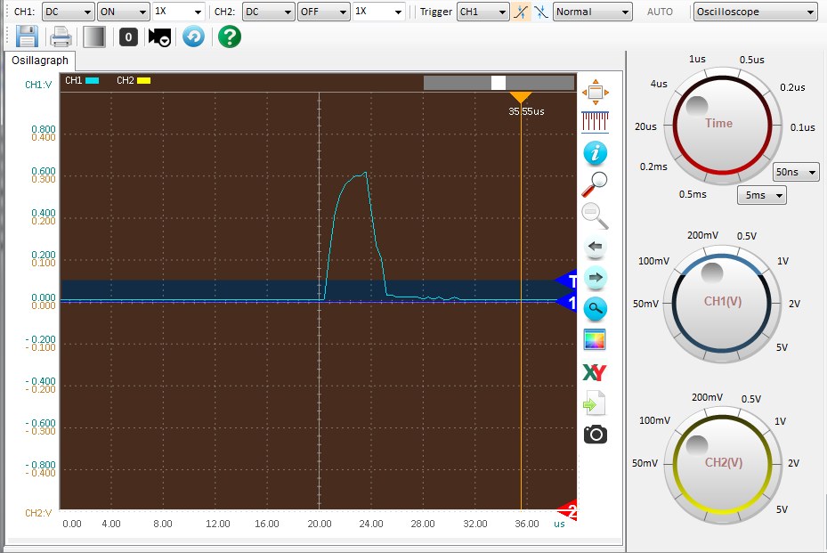
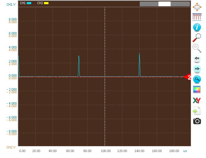
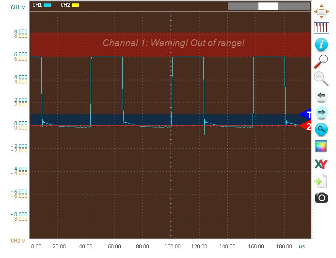
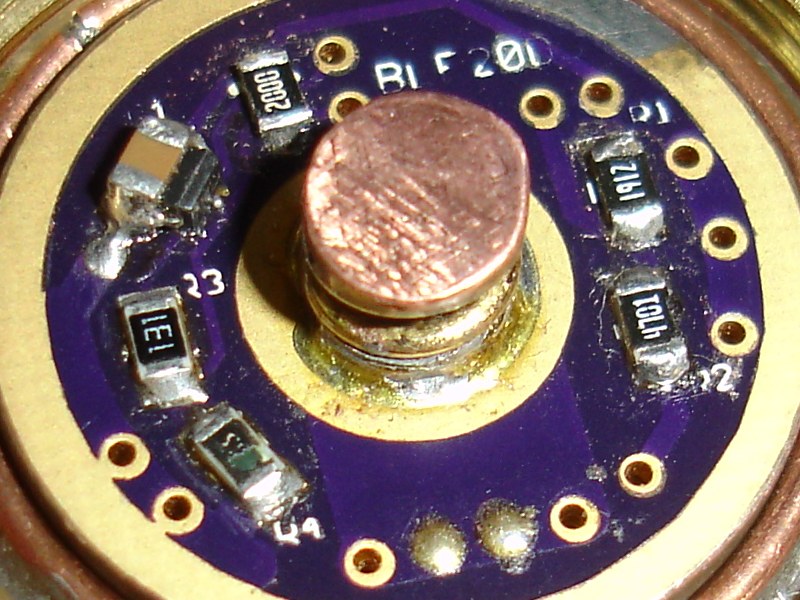
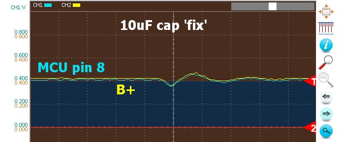
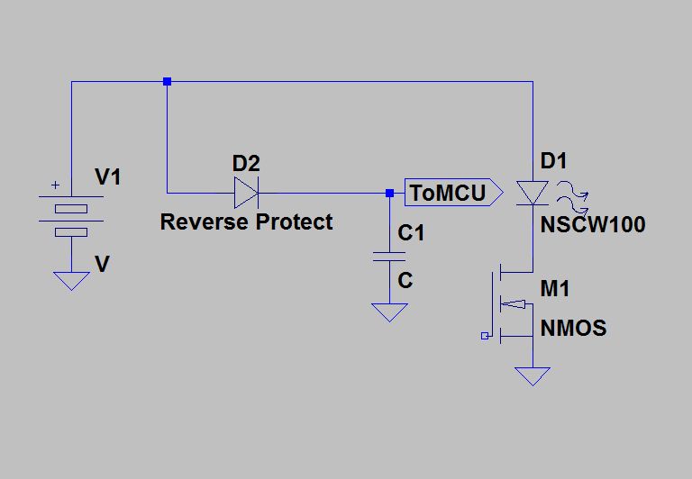
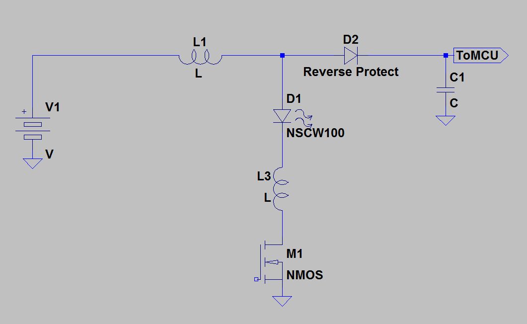
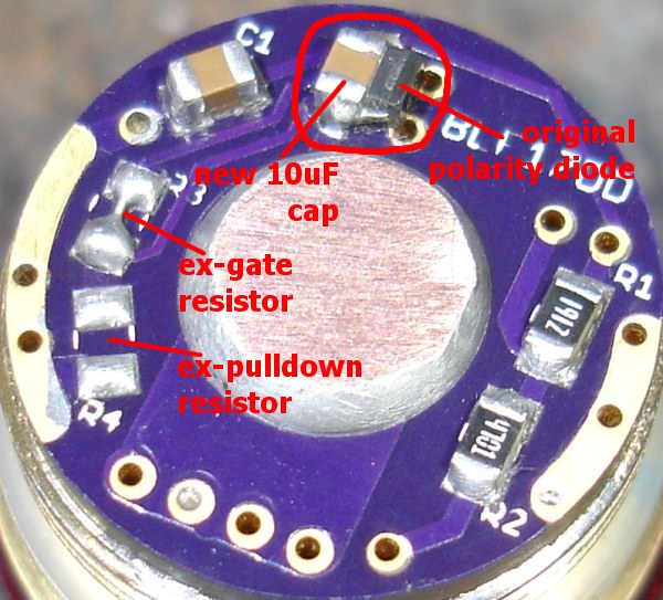
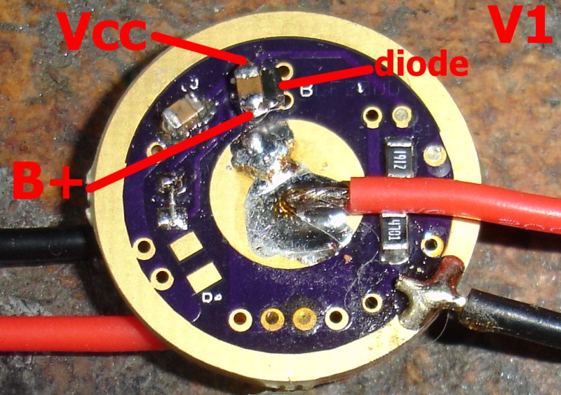
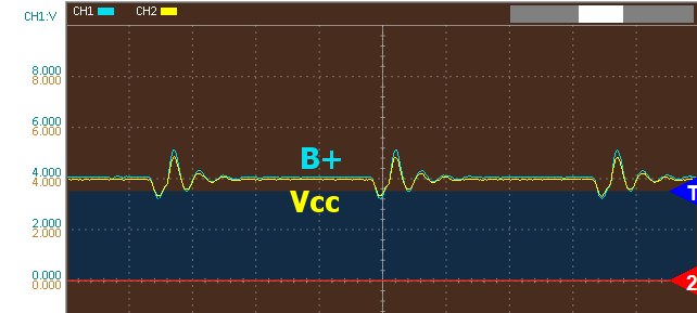
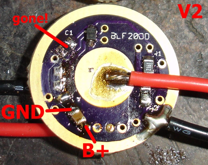
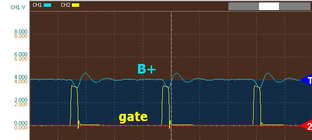
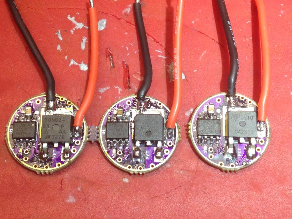
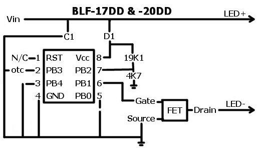
Still learning what all the buttons do so this is very preliminary. Testing on a BLF-20DD, with the known-working combo of Vishay 70N02 FET, 130 ohm gate resistor, 12K gate pulldown resistor. Using a fast-PWM build of luxdrv, I'll get to other versions eventually to see if there's a difference.

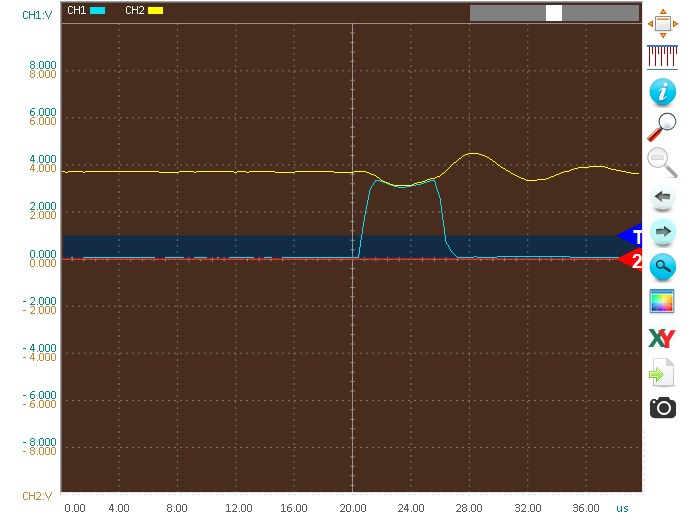
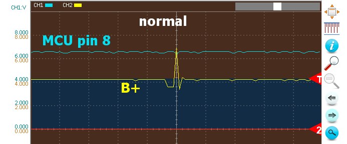
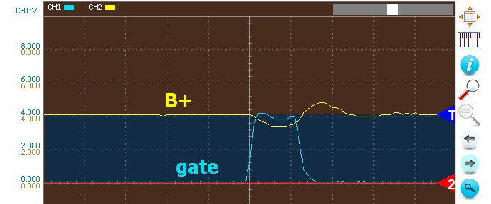
In 'low' mode (PWM value of 12), this is the waveform at the FET's gate pin with the driver running normally:

../comfychair//scope/screenshot.01-07-2014%2004.10.11.jpg

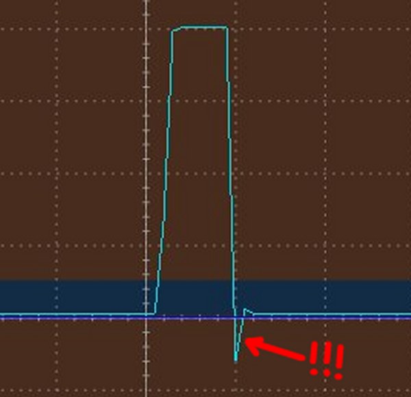
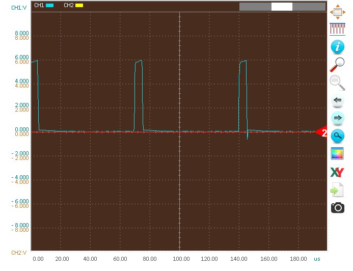
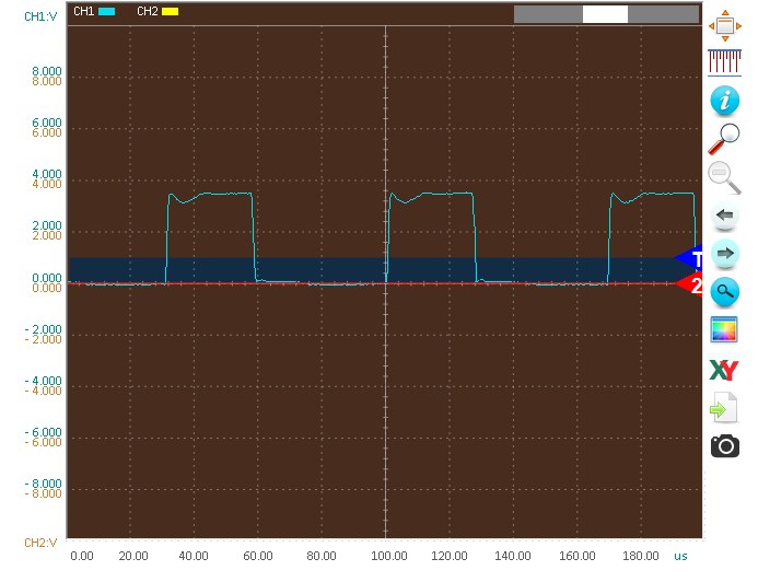
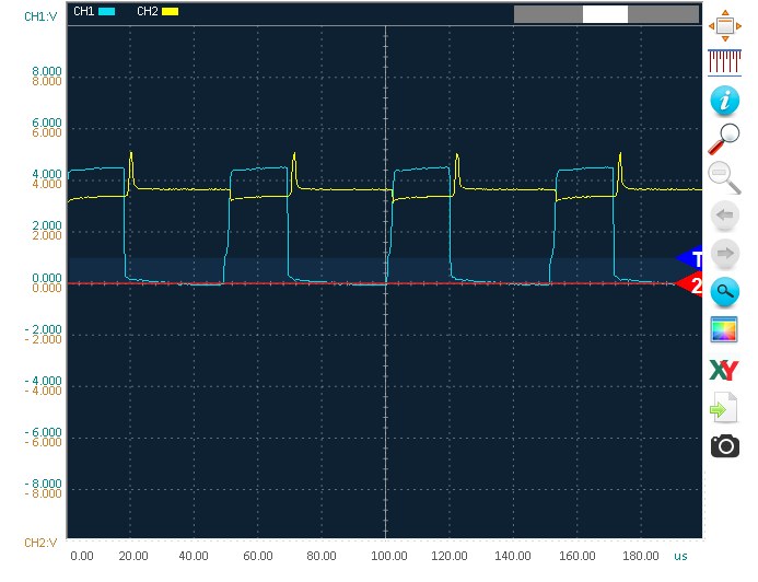
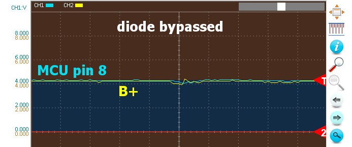
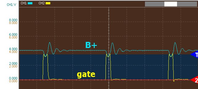
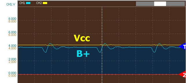
...and then, with the gate resistor jumpered (actually, just grabbed on both pads with tweezers):

../comfychair//scope/screenshot.01-07-2014%2004.09.54.jpg

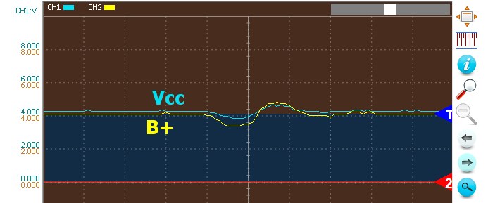
Interesting thing I wasn't expecting, the LEDs got dimmer with the gate resistor shorted. The peak at the gate is higher, but for less time. The resistor really drags it out and that leaves the FET on (or partially on) for longer, which makes more light.

__________________

...


djozz's picture
Offline
Last seen: 1 hour 12 min ago
Title: ★★★★★
Joined: 09/07/2012
Posts: 6830
Location: Amsterdam
I'm not into this electronics

I'm not into this electronics much, but it is nice to see you looking at the new drivers like this, it will help finding the right values for the components more accurately. Was the driver under load of a led? Or does that not matter in this case?

__________________

comfychair's picture
Offline
Last seen: 1 year 10 weeks ago
Title: ★★★★★
Joined: 01/12/2013
Posts: 5873
Yes, it was powered by a

Yes, it was powered by a single ICR18650-28A in a battery box (with a switch on the side), and a triple XPG2 board mounted on my test heatsink.

One thing I'll have to figure out how to investigate is that on the drivers that don't work right, they most times just shut off completely after changing modes. So there's no signal there to measure. I think it happens too quick to get anything useful from a frame capture.

I still have lots of other stuff on the to-do list: like, what does the output side look like with various hardware/firmware, and one thing I really really want to see is the output side of the SRK-DD drivers comparing with inductor to without, to finally see for real what the inductor is doing to make the low modes lower.

__________________

...


comfychair's picture
Offline
Last seen: 1 year 10 weeks ago
Title: ★★★★★
Joined: 01/12/2013
Posts: 5873
Oh, and I forgot the most

Oh, and I forgot the most important part. That bounce at the end with the resistor shorted is likely the thing that makes the drivers act goofy with no resistor or the wrong value resistor.

../comfychair//scope/bounce.jpg

__________________

...


FmC
FmC's picture
Offline
Last seen: 7 hours 24 min ago
Title: ★★★★★
Joined: 03/31/2013
Posts: 1385
Location: AU
I’m liking what you’re doing

I’m liking what you’re doing – what equipment & s/w are you using?

__________________


comfychair's picture
Offline
Last seen: 1 year 10 weeks ago
Title: ★★★★★
Joined: 01/12/2013
Posts: 5873
SainSmart DDS120.
__________________

...


comfychair's picture
Offline
Last seen: 1 year 10 weeks ago
Title: ★★★★★
Joined: 01/12/2013
Posts: 5873
This is a properly-working

This is a properly-working 20DD flashed with STAR momentary, PWM levels of 2-6-18-54-130-255, using same gate/pulldown resistors of 130/12K as before.

PWM=2

../comfychair//scope/L1-PWM2.jpg

PWM=6

../comfychair//scope/L2-PWM6.jpg

PWM=18

../comfychair//scope/L3-PWM18.jpg

PWM=54

../comfychair//scope/L4-PWM54.jpg

PWM=130

../comfychair//scope/L5-PWM130.jpg

PWM=255 (???)

../comfychair//scope/L6-PWM255.jpg

__________________

...


djozz's picture
Offline
Last seen: 1 hour 12 min ago
Title: ★★★★★
Joined: 09/07/2012
Posts: 6830
Location: Amsterdam
comfychair wrote:This is a

comfychair wrote:

This is a properly-working 20DD flashed with STAR momentary, PWM levels of 2-6-18-54-130-255, using same gate/pulldown resistors of 130/12K as before.

PWM=2

../comfychair//scope/L1-PWM2.jpg

PWM=6

../comfychair//scope/L2-PWM6.jpg

PWM=18

../comfychair//scope/L3-PWM18.jpg

PWM=54

../comfychair//scope/L4-PWM54.jpg

PWM=130

../comfychair//scope/L5-PWM130.jpg

PWM=255 (???)

../comfychair//scope/L6-PWM255.jpg

that gives a good insight in how pulse-width and PWM percentages translate in amounts of light Smile 
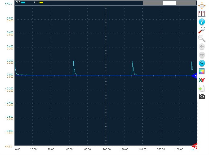
. Reminds me of HKJ's review of the qlite driver and its problems with highfreq. modulation

__________________

comfychair's picture
Offline
Last seen: 1 year 10 weeks ago
Title: ★★★★★
Joined: 01/12/2013
Posts: 5873
But remember, this is the

But remember, this is the signal fed to the gate, not the output to the LED. I suppose since I have a second channel available I could grab both sides in the same picture...

__________________

...


Werner's picture
Offline
Last seen: 6 hours 3 min ago
Title: ★★★★★
Joined: 10/19/2012
Posts: 3519
Location: Germany
Why is the voltage so low???

Why is the voltage so low???

Edit:nevermind I guess it’s a 10:1 divider in line…

I would find it interesting if the negative bump goes away if you actually short it with a small wire or solder blob. Maybe the inductance of the tweezers cause it.

ImA4Wheelr's picture
Offline
Last seen: 4 hours 25 min ago
Title: ★★★★★
Joined: 02/03/2013
Posts: 6170
Location: SC, USA
This is really great stuff. 

This is really great stuff.  Well be following this thread closely.  Thanks for reporting. 

comfychair's picture
Offline
Last seen: 1 year 10 weeks ago
Title: ★★★★★
Joined: 01/12/2013
Posts: 5873
Also remember there's a

Also remember there's a threshold for the gate voltage before any current can get through the FET. The signals don't look all that different in duration between 2 & 6 & 18 if you look at the entire thing, but if you only count roughly the part above the '0.200' line the difference is about in line with what you'd expect with those PWM levels.

__________________

...


Bucket's picture
Offline
Last seen: 5 weeks 2 days ago
Title: ★★★★
Joined: 07/19/2013
Posts: 634
Location: Altoona, PA
This is super info Comfy.

This is super info Comfy.  Great work.

__________________

“If you don't read the newspaper, you are uninformed; if you do read the newspaper, you are misinformed.” —Mark Twain

comfychair's picture
Offline
Last seen: 1 year 10 weeks ago
Title: ★★★★★
Joined: 01/12/2013
Posts: 5873
This is a different 20DD,

This is a different 20DD, same 70N02, same build of STAR momentary, but NO gate resistor (replaced with wire, soldered) and no pulldown resistor (left blank). This combo, this exact same driver, did not work using the clicky firmware. It works flawlessly with the momentary FW.

PWM=2

../comfychair//scope/noR-L1-PWM2.jpg

PWM=6

../comfychair//scope/noR-L2-PWM6.jpg

PWM=18

../comfychair//scope/noR-L3-PWM18.jpg

PWM=54

../comfychair//scope/noR-L4-PWM54.jpg

PWM=130

../comfychair//scope/noR-L5-PWM130.jpg

__________________

...


comfychair's picture
Offline
Last seen: 1 year 10 weeks ago
Title: ★★★★★
Joined: 01/12/2013
Posts: 5873
I do not understand what this

I do not understand what this is, but something tells me it is important!


20DD, 70N02, NO gate resistor (replaced with wire, soldered). When flashed with clicky firmware (either luxdrv or STAR) it occasionally goes goofy when changing modes - mostly when dropping from high to mid, other modes, if you can get to them, seem stable.

This is taken at the FET's gate pin, with everything normal:

../comfychair//scope/70N02-nogate-diodenormal.jpg

Right. We've seen that before. But then...

With the polarity protection diode bypassed, no other changes, driver still running in the same mode as the first pic, not even shut off between the two pics:

../comfychair//scope/70N02-nogate-diodebypassed.jpg

How is... I mean... what? With the diode bypassed, all mode changing happens correctly, no more weirdness. Un-short the diode and it goes back to acting flaky. The voltage scale in the first pic is likely correct - yep, 6 volts at the gate when running thru the diode like normal. But bypass the diode and the gate voltage just happens to exactly match the actual Vin. Is this a diode issue, or a capacitor issue?? Where the hell is the extra 2 volts coming from?

__________________

...


ImA4Wheelr's picture
Offline
Last seen: 4 hours 25 min ago
Title: ★★★★★
Joined: 02/03/2013
Posts: 6170
Location: SC, USA
That is real weird. 

That is real weird.  Shouldn't the diode be using up some voltage and causing lower voltage to the MCU?  I take it you made sure the screen shots were not mixed up?

comfychair's picture
Offline
Last seen: 1 year 10 weeks ago
Title: ★★★★★
Joined: 01/12/2013
Posts: 5873
The waveform with the diode

The waveform with the diode operating normally matches the other ones taken earlier on the same driver (or other drivers while bridging the gate resistor). I saw it change from the top pic to the bottom pic when I grabbed across the diode with the tweezers.  Did it multiple times while running the frame capture.

Does the location of the capacitor make a difference? Would it be 'better' on the topside of the board closer to pin #8? It just seems like it's a long way off from the thing it needs to filter.

Way back when these problems first showed up I replaced the Digikey diode with one from a 105C and it showed the same behavior, so I ruled out the diode. What I didn't ever do though was swap in a cap from a 105C.

__________________

...


comfychair's picture
Offline
Last seen: 1 year 10 weeks ago
Title: ★★★★★
Joined: 01/12/2013
Posts: 5873
Same no-resistor driver, low

Same no-resistor driver, low mode (PWM = 18). CH1 is the FET gate, CH2 is Vin measured between the B+ pad & ground ring (so, before the diode):

../comfychair//scope/gate-Vin-nocap.jpg

And this is the same but with a 470uF cap stuck between B+ and GND (also before the diode):

../comfychair//scope/gate-Vin-470uF.jpg

Stare

__________________

...


Offline
Last seen: 22 weeks 12 min ago
Title: ★★★
Joined: 04/19/2013
Posts: 455
Location: Schleswig-Holstein, Germany
Perfect example why an

Perfect example why an oscilloscope is such an invaluable tool.
One might have guessed something like that at some point, but seeing it is a quite different thing.
Leads inductance, diode and cap make a nice boost converter, don’t they? Wink

Werner's picture
Offline
Last seen: 6 hours 3 min ago
Title: ★★★★★
Joined: 10/19/2012
Posts: 3519
Location: Germany
Now we need one after the

Now we need one after the diode to check how the controller supply voltage reacts…

comfychair's picture
Offline
Last seen: 1 year 10 weeks ago
Title: ★★★★★
Joined: 01/12/2013
Posts: 5873
What do you want to see on

What do you want to see on the two channels, before diode & after diode, or after diode & gate pin?

The giant electrolytic cap I'm poking around onto various pads completely at random gives an interesting change when it's placed across the diode, too, but that's not a real-world solution to anything (it's way too big). Would a smaller SMD cap in parallel with the diode accomplish the same thing? I need to figure out a way to try that...

I also swapped our known-value 10uF/16v cap for the unknown-value part that comes on a 105C, no change... I also tried the cap on the top of the board straight from the MCU pin to ground (electrically the same, just different trace lengths) with no change, and then tried the two SMD caps at the same time, one in the original location on the battery side and a second one on top at the MCU, again no change.

Also tried the big electrolytic in the same location as the small SMD cap, no change. But putting it between B+ and GND, or in parallel with the diode, did get rid of the weird overvoltage spikes.

__________________

...


comfychair's picture
Offline
Last seen: 1 year 10 weeks ago
Title: ★★★★★
Joined: 01/12/2013
Posts: 5873
I am assuming here that this

I am assuming here that this spike thing is the cause of the mode-change issues when there's no gate resistor present, since doing anything to eliminate the spike (bypassing the diode, or adding the cap between B+/GND) also eliminated the mode-change issues. Am I at least on the right track? That the solution is something practical that eliminates the voltage spike?

__________________

...


Werner's picture
Offline
Last seen: 6 hours 3 min ago
Title: ★★★★★
Joined: 10/19/2012
Posts: 3519
Location: Germany
Like you know I also have

Like you know I also have often this problem, just put a normal nanjg in my t08 because my test driver with some smd FETs in parallel was gone crazy…
I also tried to add caps in some different capacities(sometimes stacked half a dozen), resistors and stuff everywhere but couldn’t get a valid explanation or solution. I am happy that you try to analyze these issues:)
————————————————
If I am right that is our hypothesis:
That the controller behaves sometimes strange and what often can get wiped out with a big cap is in my eyes also a problem with the controller input voltage, because every time the FET switches it is like a short….
The idea behind the diode is that the led can’t discharge the cap behind the diode and so the controller always has enough voltage to work also in the switching phase.
A cap between the bat- and bat+ buffers this also but because it gets discharged through the led with serious amps it needs to be a big one.
Now the only reasonable guess would be that this voltage protection isn’t working as we think.
——————————————————

I just want to see if that diode and cap construct works to smoothen the power supply or if the controller also sees these spikes, because I think that has to be the problem…??? So both would be interesting controller voltage and FET signal, so that we can see if there is a correlation between the switching and the power. Also the before and after diode is interesting to see if it actually works like we think it will.

comfychair's picture
Offline
Last seen: 1 year 10 weeks ago
Title: ★★★★★
Joined: 01/12/2013
Posts: 5873
What has me confused is

What has me confused is here:

../comfychair//scope/gate-Vin-nocap.jpg

(same pic from post #18 - trigger here is on the rising edge of CH1 (gate signal) at 1.00v, that's close to the FET's threshold voltage)

I can (mostly) understand the spike on CH2 after the PWM turns off. What I don't get is how the gate voltage rises to ~6v, and stays there, while the supply to the MCU is still down at battery voltage. If they tracked together more closely it wouldn't be much of a mystery. The ~6v being generated when it turns off, sure. Removing the load, it releases stored energy in the cap, and voltage spikes. But it's doing a constant, rock steady 6v output to the gate pin while input to the MCU is still down at ~3.9v.

__________________

...


Werner's picture
Offline
Last seen: 6 hours 3 min ago
Title: ★★★★★
Joined: 10/19/2012
Posts: 3519
Location: Germany
These spikes always are

These spikes always are generated when switching an inductance, all these switching and the diode+cap leads to the high voltage. Every spike gets over the diode to charge the cap at a higher voltage but never gets discharged down to the supply voltage again. You have to imagine there are a lot of these spikes and the controller don’t use much power so the voltage don’t breaks in.
Like someone said its a boost circuit.
Ch2 is not input of mcu because there is a diode between your measuring point and the controller and the diode prevents current flowing in that direction. If you measure the controller voltage I am sure we will see the 6V supply…

Maybe we have a overvoltage problem and no undervoltage problem? Do these problems also occur on Zener modded nanjgs?

comfychair's picture
Offline
Last seen: 1 year 10 weeks ago
Title: ★★★★★
Joined: 01/12/2013
Posts: 5873
I haven't looked at any of

I haven't looked at any of this on a zener-modded driver yet, I don't have one built at the moment...

Do you have a prediction as to what the scope will show with a 10uF SMD cap in parallel with the polarity diode?

__________________

...


Werner's picture
Offline
Last seen: 6 hours 3 min ago
Title: ★★★★★
Joined: 10/19/2012
Posts: 3519
Location: Germany
The parallel cap sees the

The parallel cap sees the voltage spike on both legs so it shouldn’t get so charged up like the stock one. Only the diode forward voltage should be between the two legs. I guess that compensates the spike and stabilize because there is then a cap in both directions: one from controller+ to GND and one from controller+ to V+. So the “negative” side of the cap is the V+ side….
But this are only unfunded fantasies….

Have you never used a Zener modded FET driver? Never thought about that but now I need to go the the soldering iron….and test some things.

Atmel rates the maximum Voltage for the tiny at 5.5V.

comfychair's picture
Offline
Last seen: 1 year 10 weeks ago
Title: ★★★★★
Joined: 01/12/2013
Posts: 5873
Yes, I've built lots of them,

Yes, I've built lots of them, I just don't have one put together right now. Have plenty of parts on hand to build them.

Torchlite SVD7 MTG2 built for DayLighter:

../comfychair//Dsc07910.jpg

__________________

...


comfychair's picture
Offline
Last seen: 1 year 10 weeks ago
Title: ★★★★★
Joined: 01/12/2013
Posts: 5873
Another 10uF/16v cap placed

Another 10uF/16v cap placed at D1, with the diode piggybacked:

../comfychair//scope/Dsc08268.jpg

CH1 = gate, CH2 = VBAT

../comfychair//scope/CH1-gate_CH2-VBAT.jpg

CH1 = gate, CH2 = MCU's Vcc, pin 8:

../comfychair//scope/CH1-gate_CH2-Vcc.jpg

__________________

...


comfychair's picture
Offline
Last seen: 1 year 10 weeks ago
Title: ★★★★★
Joined: 01/12/2013
Posts: 5873
comfychair wrote:The ~6v

comfychair wrote:

../comfychair//scope/gate-Vin-nocap.jpg

The ~6v being generated when it turns off, sure. Removing the load, it releases stored energy in the cap, and voltage spikes.

The weird behavior of some drivers without a gate resistor, where the MCU seems to shut down right after changing modes, is likely due to the overvoltage to the MCU from that spike. It's doing exactly what it seems like, it's shutting itself down! It sees that ~6v and says 'whoa dude, I need a little nap - wake me up when shit gets back to normal.'

__________________

...


comfychair's picture
Offline
Last seen: 1 year 10 weeks ago
Title: ★★★★★
Joined: 01/12/2013
Posts: 5873
So how did adding the stupid

So how did adding the stupid gate resistor cover up this issue - just by reducing the load the MCU has to drive, therefore reducing the current draw through the diode, which reduced the tendency to create the voltage spike?

__________________

...


WarHawk-AVG's picture
Offline
Last seen: 17 hours 16 min ago
Title: ★★★★★
Joined: 01/04/2014
Posts: 4873
Location: H-Town
So by putting in the cap, the

So by putting in the cap, the load resistor can go away?

comfychair's picture
Offline
Last seen: 1 year 10 weeks ago
Title: ★★★★★
Joined: 01/12/2013
Posts: 5873
Correct, the 100-130 ohm gate

Correct, the 100-130 ohm gate resistor no longer needed.

Also, due to the different circuit layout of the zener-mod drivers, those don't suffer the same voltage spike, so don't need any changes. Unless it's one of the zener-specific boards that are designed to keep a polarity protection diode. I don't know if any are, I haven't looked at them that closely. But a normal driver converted with a resistor in place of the diode, and the zener in parallel with the cap, isn't going to be able to generate these spikes. Those drivers likely never needed the gate resistor in the first place.

__________________

...


Online
Last seen: 3 min ago
Title: ★★★★★
Joined: 11/27/2013
Posts: 4411
Location: Virginia, USA
Do you have a East-92 to

Do you have a East-92 to compare? As I said earlier in post #987 here, the diode is likely being used to help with this problem. I could certainly be wrong, but I suspect that the diode may work better. Once the cap is charged/discharged it maxes out. Bigger caps will have diminishing returns & high costs. The diode will continue conducting to remove our stray voltage until Vf is reached.

Good work so far.

Online
Last seen: 3 min ago
Title: ★★★★★
Joined: 11/27/2013
Posts: 4411
Location: Virginia, USA
comfychair wrote:So how did

comfychair wrote:

So how did adding the stupid gate resistor cover up this issue – just by reducing the load the MCU has to drive, therefore reducing the current draw through the diode, which reduced the tendency to create the voltage spike?

The resistor softens the turn-off. The sharp turn-off is what causes the spike. The purpose of the diode as I understand it is give the spike a path to escape through rather than shoving itself where we don’t want it.

comfychair's picture
Offline
Last seen: 1 year 10 weeks ago
Title: ★★★★★
Joined: 01/12/2013
Posts: 5873
I'm posting stuff all over

I'm posting stuff all over the place, these two were in the Oshpark thread.

Stock 105C hardware, CH1 on Vdd (MCU pin 6), CH2 on B+ before the diode:

../comfychair//scope/stock105C.jpg

Battery voltage was well below 4v for that pic.

This is a 20DD, no gate resistor, but otherwise using the original parts in the original spots (without the add-on capacitor across the diode). CH1 is after the diode (MCU pin 8 EIGHT, stupid auto-smiley crap), CH2 is before the diode (B+). Battery voltage was around 4.08v no-load.

../comfychair//scope/CH1-VBAT_CH2-Vcc_diodenormal.jpg

Look at that beautiful flat line for CH1... if only it weren't way up there at 6 volts. 6 volts!!


I have one east-092 but it's one of the crap versions. I have dead stuff I can scavenge parts from, where should the diode go - between LED+ and LED-?

__________________

...


Online
Last seen: 3 min ago
Title: ★★★★★
Joined: 11/27/2013
Posts: 4411
Location: Virginia, USA
comfychair wrote:I’m posting

comfychair wrote:

I’m posting stuff all over the place, these two were in the Oshpark thread.

Stock 105C hardware, CH1 on Vdd (MCU pin 6), CH2 on B+ before the diode:

Battery voltage was well below 4v for that pic.

This is a 20DD, no gate resistor, but otherwise using the original parts in the original spots (without the add-on capacitor across the diode). CH1 is after the diode (MCU pin 8 EIGHT, stupid auto-smiley crap), CH2 is before the diode (B+). Battery voltage was around 4.08v no-load.

Look at that beautiful flat line for CH1… if only it weren’t way up there at 6 volts. 6 volts!!


It seems that voltage is not always accurately depicted. In your trace with the Stock 105C hardware Vdd is shown >4v, this is not accurate if B+ is <4v. Actual Vdd will be much lower, the combined effects of the protection diode, B+ drop under load, and the ATtiny13A’s hardware should put Vdd closer to 3.0v I’d estimate?

comfychair wrote:

I have one east-092 but it’s one of the crap versions. I have dead stuff I can scavenge parts from, where should the diode go – between LED+ and LED-?

Yes, but the anode and cathode will be backwards compared to the LED.

comfychair's picture
Offline
Last seen: 1 year 10 weeks ago
Title: ★★★★★
Joined: 01/12/2013
Posts: 5873
If I use the scope probes to

If I use the scope probes to check the battery voltage, it matches what my DVOM says. And when I add the capacitor in parallel with the diode, the gate voltage no longer goes above battery voltage - the 'boost circuit' is effectively disabled (or at least severely impaired). Shorting across the diode also gets rid of the overvoltage on all 3 spots - gate, Vcc, & B+.

edit: see post #14 for a comparison of diode normal vs. diode shorted, gate voltage drops to battery voltage just by shorting the diode

__________________

...


Online
Last seen: 3 min ago
Title: ★★★★★
Joined: 11/27/2013
Posts: 4411
Location: Virginia, USA
For clarity I am referring to

For clarity I am referring to the trace shown in post #35. I realize that you have it in quotes, but there is no ‘boost circuit’. The ATtiny is completely incapable of providing an output higher than it’s input. Vdd is the enable pin on a 7135, the 7135 definitely does not increase the voltage of that pin beyond what the ATtiny puts there. The trace clearly show that the voltage is constant across the pulse, it is not a spike. The battery voltage is clearly shown as lower than the Vdd voltage. All I’m saying is that that is definitely incorrect. Where did you attach your ground clips?

EDIT: see dave_’s post #47 & #50 in this thread. He explains clearly why what I wrote in this post is wrong. (in other words there does appear to be an unwanted boost circuit created by our component layout)

comfychair's picture
Offline
Last seen: 1 year 10 weeks ago
Title: ★★★★★
Joined: 01/12/2013
Posts: 5873
Tried a diode (axial IN5817

Tried a diode (axial IN5817 schottky) between LED +&-, absolutely zero effect on either the waveforms or on correct mode changing.

This is the 20DD again. No gate resistor.

../comfychair//scope/screenshot.04-07-2014%2015.55.53.jpg

../comfychair//scope/screenshot.04-07-2014%2015.56.08.jpg

../comfychair//scope/screenshot.04-07-2014%2016.05.54.jpg

__________________

...


Cereal_killer's picture
Offline
Last seen: 8 weeks 4 days ago
Title: ★★★★★
Joined: 07/22/2013
Posts: 2955
Location: Columbus, OH USA Earth
I have to build 2 BLF drivers

I have to build 2 BLF drivers later on today, I’ll definitely be trying this out on them. Because it removes the gate resistor it should make low slightly lower right?

Thanks for all the work, I’m trying to finish up a few lights to make some money to buy one of those same oscilloscopes now that I see yours, I’d never seen them before. One thing I’m interested in looking at is the 1/2 off mode using Werners UI when using a long press to turn the light off from low (like in the video I showed you)

__________________

Please help support my research by giving or sharing. GoFundMe.com/DansDrones


Always remember SPC Joey Riley, KIA 11/24/14.

comfychair's picture
Offline
Last seen: 1 year 10 weeks ago
Title: ★★★★★
Joined: 01/12/2013
Posts: 5873
Well, without the resistor

Well, without the resistor you can use a lower minimum PWM value, the resistor raises the point at which the LEDs will start making light. I guess one way of saying it (probably wrong, but...) is that the gate resistor reduces the resolution at the low end.

__________________

...


Online
Last seen: 3 min ago
Title: ★★★★★
Joined: 11/27/2013
Posts: 4411
Location: Virginia, USA
comfychair wrote:Tried a

comfychair wrote:

Tried a diode (axial IN5817 schottky) between LED +& – , absolutely zero effect on either the waveforms or on correct mode changing.

This is the 20DD again. No gate resistor.

Hmm, interesting. Thanks for trying it. All 3 pictures in post #39 are with a 20DD board which has the IN5817 installed between LED+/-?

comfychair's picture
Offline
Last seen: 1 year 10 weeks ago
Title: ★★★★★
Joined: 01/12/2013
Posts: 5873
I could have made copies of

I could have made copies of each of the 3 pics and given them different names to differentiate between with output diode and without, because they look absolutely the same either way. Tongue 
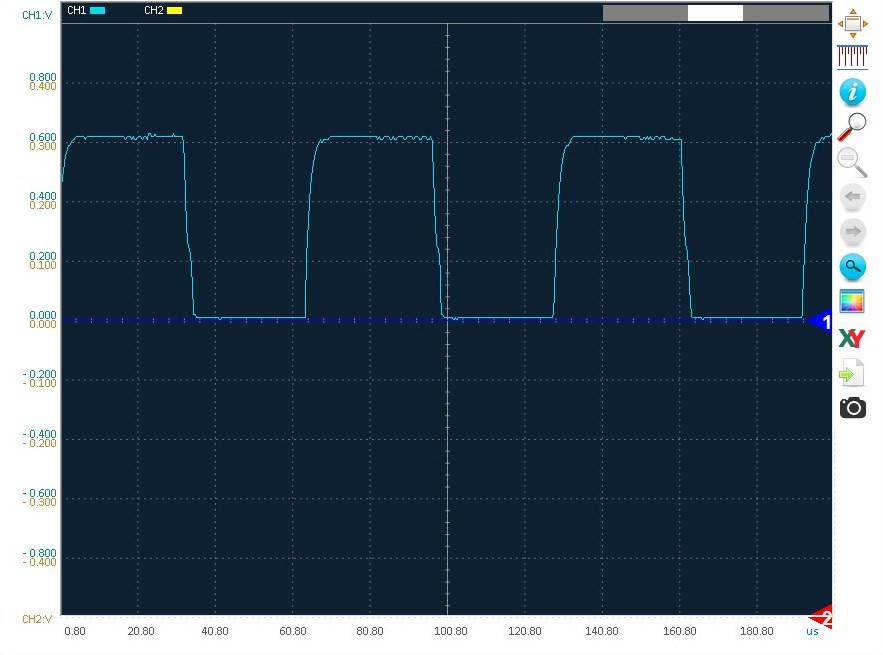
(and it still wouldn't change modes right, and so far I haven't seen anything that will fix the glitchy mode changing issue that doesn't also fix the over-voltage thing)

Yes, same driver in all 3. From pic 1 to pic 2 it wasn't even shut off, I just stuck a wire onto both legs of the polarity protection diode while it was running. Then for pic 3 I removed the diode, added the cap in its place, and stuck the diode back on. The wires in and out and the scope probes weren't even disconnected for any of it.

This driver previously wouldn't work without the gate resistor, after adding the cap and removing the resistor it runs perfect:

../comfychair//driverhacks/BLF-17DD-capfix.jpg

__________________

...


Online
Last seen: 3 min ago
Title: ★★★★★
Joined: 11/27/2013
Posts: 4411
Location: Virginia, USA
comfychair wrote:I could have

comfychair wrote:

I could have made copies of each of the 3 pics and given them different names to differentiate between with output diode and without, because they look absolutely the same either way. Tongue (and it still wouldn’t change modes right, and so far I haven’t seen anything that will fix the glitchy mode changing issue that doesn’t also fix the over-voltage thing)

Yes, same driver in all 3. From pic 1 to pic 2 it wasn’t even shut off, I just stuck a wire onto both legs of the polarity protection diode while it was running. Then for pic 3 I removed the diode, added the cap in its place, and stuck the diode back on. The wires in and out and the scope probes weren’t even disconnected for any of it.

This driver previously wouldn’t work without the gate resistor, after adding the cap and removing the resistor it runs perfect:

Tongue

  1. Your B+ trace is generated with the probe stuck where? Directly on the B+ contact pad I assume?
  2. The difference we see from bypassing the polarity protection diode is what’s really intriguing me right now.
  3. The IN5817 was attached between BAT+ and the FET’s tab with the bar facing BAT+, right? Just confirming.
comfychair's picture
Offline
Last seen: 1 year 10 weeks ago
Title: ★★★★★
Joined: 01/12/2013
Posts: 5873
1. Yes... actually, the wire

1. Yes... actually, the wire soldered to the + pad I intentionally left with enough exposed wire for the probe to clip onto. So it's about, what, 1mm or less from the pad? For pics showing the gate signal, I clip the probe directly onto the FET's leg. For the MCU pin 8 signal I remove the grabber attachment and use the pointy end and hold it on the pin. Probe grounds are clipped onto the driver's ground ring.

2. Me too, dude. dave_ said earlier that this particular combo of wire length*, capacitor (C1), and diode (D1) is creating a (very) crude boost circuit. There's no single component anywhere that is on purpose generating boosted voltage, I never thought that was the case... but 6V input on pin 8 results in, unsurprisingly, 6V output on pin 6. Whatever fix it takes to get pin 8 down to the actual B+ voltage is what will fix the erratic behavior. (completely removing the diode isn't a solution even if losing reverse polarity stuff would be acceptable, cause it screws up voltage monitoring and also the driver can't be reflashed unless the jumper across D1 is removed, it gives 'no communication...' otherwise. Other than all that, eliminating the diode would be the most simple fix, but not at all practical.)

3. Yup. It did so much of nothing I even reversed it, where of course it shut off the LEDs. Innocent


*The wire length can't be contributing all that much, since the drivers that act goofy on the bench also still act goofy when installed in a light.

__________________

...


comfychair's picture
Offline
Last seen: 1 year 10 weeks ago
Title: ★★★★★
Joined: 01/12/2013
Posts: 5873
As if I need more

As if I need more unexplainable stuff to throw on the pile, I have one really strange one. I have a BLF-SRK driver that has always run fine on all kinds of cells (INR 20R & 25R, Panasonic ICR 2900s), but absolutely freaks out and refuses to change modes or shuts off completely if I put in four Samsung ICR 28As (only charged to 4.20v, never tried with full charge to 4.30). I did the same extra 10uF capacitor trick on it, and it now runs perfect on the 28As. Puzzled

__________________

...


Offline
Last seen: 22 weeks 12 min ago
Title: ★★★
Joined: 04/19/2013
Posts: 455
Location: Schleswig-Holstein, Germany
With a big current change in

With a big current change in a very short time, you don’t need all that much inductivity to charge a small cap to 6V. And if the mcu + fet drive takes less charge than the spike puts in, it will stay there forever. Smile
With your quite hard switching (high slope), that’s what you get. Tongue

Since i’m on limited mobile traffic I won’t go searching for the actual circuit, but with ‘dd’
and ‘reverse protection diode’, I imagine it somewhat like that:

When we draw in some of the parasitic inductance, it looks somewhat like that:

There is your booster. Wink

To get rid of the effect there are several options:
-soften the switching (gate resistor)
-clamp voltage at mcu with suppressor diode (5.5V types should be available plenty)
-add snubber circuit to dampen the spike (in some way like your big el. cap now does)

I’d probably try softer switching and one of the others. Whatever the easiest/cheapest is.

Werner's picture
Offline
Last seen: 6 hours 3 min ago
Title: ★★★★★
Joined: 10/19/2012
Posts: 3519
Location: Germany
Congratulation you have found

Congratulation you have found the problem, never have thought of overvoltage until now. Party
Thanks for the pics in #39.
That is what I wanted to see. But I am a bit surprised that there is no spike in the diode bypassed picture…?

@dave we know why it is but why does a cap over the diode help…?

comfychair's picture
Offline
Last seen: 1 year 10 weeks ago
Title: ★★★★★
Joined: 01/12/2013
Posts: 5873
Oh no, I only used the big

Oh no, I only used the big cap because it was at hand and easy to make contact with various points while watching the scope. I'm using an 0805 10uF/16V X7R, same part as the Nanjg's capacitor (and same as used on the BLF boards at C1). Are there any longevity/performance worries with doing it this way? It definitely does cure the problems that come from not using the gate resistor.

../comfychair//driverhacks/BLF-17DD-capfix-annotated.jpg

../comfychair//scope/CH1-gate_CH2-Vin_10uF.jpg

../comfychair//scope/CH1-Vcc_CH2-Vin_10uF.jpg

It's not perfect but if it fixes the problem, does it matter...?

__________________

...


Offline
Last seen: 22 weeks 12 min ago
Title: ★★★
Joined: 04/19/2013
Posts: 455
Location: Schleswig-Holstein, Germany
@werner parallel to the

@werner
parallel to the diode? We have not pure DC here, so current could flow through a cap back.

Since I am supposed to do work I really don’t want to, let’s look at it with spice. Laughing out loud

Here the circuit with the problem:

Now with cap in parallel:

looks familiar? Wink
See the red curve, the current through the cap.

Here the falling edge zoomed in. (the cap current in blue is inverted. When it is negative, current flows to the mcu cap)
You can see how the mcu voltage (red) follows the voltage before the diode/cap (grey).
As soon as the voltage before the cap changes, current flows through the cap and the voltage behind the cap also changes. Works in both directions.
The ringing is just resonance with the inductor.
So, yeah, ac can get through a cap, probably sounds familiar too. Wink

@comfychair
Well, if the cap has a half decent ripple current rating, it’s going to be fine.
It certainly is not a perfect solution with all that crap at the mcu vcc,
but that does not mean it is not a good enough and practical one. Wink

Online
Last seen: 3 min ago
Title: ★★★★★
Joined: 11/27/2013
Posts: 4411
Location: Virginia, USA
Good work everyone. Dave’s

Good work everyone. Dave’s info makes sense to me now. From his description (& spice sim) it seems that having a cap after the protection diode is integral to the unwanted boost circuit. What if we just move that input smoothing cap to before the protection diode? I’m pretty certain that’s not a perfect fix, but it seems to me that it would eliminate the boost circuit and just leave whatever remains of the spikes, similar to the diode bypass.

comfychair wrote:

1. Yes… actually, the wire soldered to the + pad I intentionally left with enough exposed wire for the probe to clip onto. So it’s about, what, 1mm or less from the pad? For pics showing the gate signal, I clip the probe directly onto the FET’s leg. For the MCU pin 8 signal I remove the grabber attachment and use the pointy end and hold it on the pin. Probe grounds are clipped onto the driver’s ground ring.

2. Me too, dude. dave_ said earlier that this particular combo of wire length*, capacitor (C1), and diode (D1) is creating a (very) crude boost circuit. There’s no single component anywhere that is on purpose generating boosted voltage, I never thought that was the case… but 6V input on pin 8 results in, unsurprisingly, 6V output on pin 6. Whatever fix it takes to get pin 8 down to the actual B+ voltage is what will fix the erratic behavior. (completely removing the diode isn’t a solution even if losing reverse polarity stuff would be acceptable, cause it screws up voltage monitoring and also the driver can’t be reflashed unless the jumper across D1 is removed, it gives ‘no communication…’ otherwise. Other than all that, eliminating the diode would be the most simple fix, but not at all practical.)

3. Yup. It did so much of nothing I even reversed it, where of course it shut off the LEDs. Innocent


*The wire length can’t be contributing all that much, since the drivers that act goofy on the bench also still act goofy when installed in a light.

Thanks comfychair. Of course that all checks out. As you know I like to make sure I’ve got a handle on the situation – detailed responses help with that. Based on what I know now I guess I’d better throw some strike-thru in a previous post Wink.

comfychair's picture
Offline
Last seen: 1 year 10 weeks ago
Title: ★★★★★
Joined: 01/12/2013
Posts: 5873
wight wrote:Good work

wight wrote:
Good work everyone. Dave's info makes sense to me now. From his description (& spice sim) it seems that having a cap after the protection diode is integral to the unwanted boost circuit. What if we just move that input smoothing cap to before the protection diode? I'm pretty certain that's not a perfect fix, but it seems to me that it would eliminate the boost circuit and just leave whatever remains of the spikes, similar to the diode bypass.

Would that cap location work? It would just go from B+ to GND. It would be easy to try anyway. I do know the driver won't run AT ALL with the cap completely removed, but I never tried just a single cap from B+ to GND.

What about... using the zener/resistor regulator, even for the 4.2v drivers? That still provides reverse polarity protection, right? How would low voltage detection be affected, with a resistor in place of the D1 diode and zener between after the resistor and GND? That would effectively dump any excess voltage to ground (though very small current based on the resistor used). Or would that setup not generate the high voltage in the first place? I don't think I've ever tried a zener-modded driver in a single-cell layout...

Or is this second capacitor idea good enough? I mean, it looks better on the scope than even a totally stock 105C, right?


(Something that hit me last night, I worried that this cap+diode thing would screw up low voltage detection - pin 8 is now 2 whole volts lower than before, but I haven't compared what's present at pin 7 between the before-mod and after-mod drivers. I did a quickie check with a used CR123 and it steps down the same in the after-mod driver as it does with the same CR123 in a light with a before-mod driver. So if it's different, it's not vastly different.)

__________________

...


Offline
Last seen: 22 weeks 12 min ago
Title: ★★★
Joined: 04/19/2013
Posts: 455
Location: Schleswig-Holstein, Germany
So, there is no cap from b+

So, there is no cap from b+ to gnd?
I’d try that then first. But keep the diode and vcc cap, just add one there.
With a little luck that’s good enough.

Online
Last seen: 3 min 1 sec ago
Title: ★★★★★
Joined: 11/27/2013
Posts: 4411
Location: Virginia, USA
dave_ wrote:So, there is no

dave_ wrote:
So, there is no cap from b+ to gnd?
I’d try that then first. But keep the diode and vcc cap, just add one there.
With a little luck that’s good enough.

Correct. There is only one cap in the stock BLF20DD circuit, it is placed after the reverse voltage protection diode. Is there a simple explanation of how this cap would be less effective if placed before the diode?

comfychair wrote:

Would that cap location work? It would just go from B+ to GND. It would be easy to try anyway. I do know the driver won’t run AT ALL with the cap completely removed, but I never tried just a single cap from B+ to GND.

What about… using the zener/resistor regulator, even for the 4.2v drivers? That still provides reverse polarity protection, right? How would low voltage detection be affected, with a resistor in place of the D1 diode and zener between after the resistor and GND? That would effectively dump any excess voltage to ground (though very small current based on the resistor used). Or would that setup not generate the high voltage in the first place? I don’t think I’ve ever tried a zener-modded driver in a single-cell layout…

Or is this second capacitor idea good enough? I mean, it looks better on the scope than even a totally stock 105C, right?


(Something that hit me last night, I worried that this cap+diode thing would screw up low voltage detection – pin 8 is now 2 whole volts lower than before, but I haven’t compared what’s present at pin 7 between the before-mod and after-mod drivers. I did a quickie check with a used CR123 and it steps down the same in the after-mod driver as it does with the same CR123 in a light with a before-mod driver. So if it’s different, it’s not vastly different.)

dave_ has probably pointed out the proper way to do this in post #53. I haven’t fully thought out what happens if you move the Vcc cap like I described in post #51. I figured that as long as the cap was still close to the ATiny it would still be able to filter for Vcc, and as long as we moved it to before the diode it would no longer form the unwanted boost circuit. Maybe dave_ can explain why part of that thinking is flawed? Until he shoots a big hole in my thought process I’d love for you to try it both ways if you want Wink.

In terms of the effect on voltage monitoring… yeah, looks like it would be affected on any drivers that sample battery voltage after the protection diode. Drivers which hook the divider up directly to B+ are unaffected. Do you get 6v on Vcc in every mode, or does the voltage of the boost circuit vary depending on PWM freq?

On the matter of whether what you’ve already done is good enough – I do not know. I’m not a guru on this stuff, but it seems unconventional. If we can get better results with a conventional method I see no reason not to do it. If just moving the Vcc cap worked and was acceptable that would lower part count. It seems that this would be an unconventional solution as well though.

As to your experience in post #46 with w/ the ICR 28A’s producing the problem and the other cells not doing it… I’d immediately assume it’s higher Internal Resistance. The higher the internal resistance of a cell, the higher voltage will spike in a scenario like this.

comfychair's picture
Offline
Last seen: 1 year 10 weeks ago
Title: ★★★★★
Joined: 01/12/2013
Posts: 5873
  Wow. Never figured that

../comfychair//scope/V1.jpg

../comfychair//scope/V1-BAT-Vcc.jpg

../comfychair//scope/V1-BAT-gate.jpg


../comfychair//scope/V2.jpg

../comfychair//scope/V2-BAT-Vcc.jpg

../comfychair//scope/V2-BAT-gate.jpg

Wow. Never figured that would have worked, because otherwise why would the 105C have the cap after the diode?

__________________

...


Online
Last seen: 3 min 1 sec ago
Title: ★★★★★
Joined: 11/27/2013
Posts: 4411
Location: Virginia, USA
Good work! Traditionally

Good work!

Traditionally that cap should be as close to VCC as possible. Putting it after the diode helps achieve that goal and doesn’t cause the original 105c circuit to malfunction (even if it makes the ATtiny operate out of spec). I’d assume that the original 105c was never modeled in SPICE or anything.

Werner's picture
Offline
Last seen: 6 hours 3 min ago
Title: ★★★★★
Joined: 10/19/2012
Posts: 3519
Location: Germany
The cap after diode is made

The cap after diode is made to buffer the voltage for the Controller which works perfect as we can see a bit to perfect as it never gets discharged and stays at 6V….(post#39)
Cap between – and + will get discharged through the led if voltage breaks in and so its Not so steady DC which can lead to some Controller malfunctions.

The Zener mod to a standard mounted driver should be the best possibility, but would need extra parts.

——-
Voltage protection is no problem because we flash the firmware by ourself anyway, the adc value just needs to be adjusted in the software, which I do anyway because I want a bit higher protection anyway… I always try the driver on a power supply if it works because the internal voltage from the ADC isn’t super accurate, but until now I never found a big mistake. I am also unsure if the voltage drop on the diode is 0.25V because the voltage only drops if current flows and there is just little current flowing, maybe you can measure it with the oscisoftware.
I have an excel sheet for easy calculating different values and get a clue which values are useful, you just fill in the resistors used and the voltage you want the protection kick in and the sheet says the value to select.

Online
Last seen: 3 min 1 sec ago
Title: ★★★★★
Joined: 11/27/2013
Posts: 4411
Location: Virginia, USA
Werner is correct. If we go

Werner is correct. If we go with the latest change (“V2” pic) the a new PCB layout should be made to push the diode and the cap very close to the VCC on the ATtiny. That way it will still be a decoupling cap (I think). As it stands it happens to work, which is good, but I think it would be hard to call that cap a decoupling cap anymore.

FWIW you never posted pictures or results from dave_’s suggestiong (post#53). He recommended keeping C1 in place and adding a cap like you did in your “V2” picture. I’m not sure exactly how that would pan out.

EDIT: Well, I want to clarify what I’m saying. I don’t think it’s normal for a decoupling cap’s operation to depend on a diode, so if Werner is saying that the cap must have a diode to keep the LED from pulling it down I don’t know if I agree with that. All I’m saying (all I know to say Wink ) is that for the cap to be effective it must be as close to the VCC pin as possible.

comfychair's picture
Offline
Last seen: 1 year 10 weeks ago
Title: ★★★★★
Joined: 01/12/2013
Posts: 5873
Cap moved from C1 to

Cap moved from C1 to B+/GND:

../comfychair//scope/V2-BAT-Vcc.jpg


1 cap at C1, 1 cap at B+/GND:

../comfychair//scope/V2.1_BAT_Vcc.jpg

Adding a cap back at C1 also brings back a little bit of boosting, Vin was below 4v for those pics and Vcc is up above that.

Voltage at pin 7, for voltage monitoring, is nice and flat with either setup (and even in the first config, with the voltage boosting and spikes and the rest). If it's stable and doesn't misbehave with just a single cap relocated, does the oscillation on Vcc hurt anything?

__________________

...


comfychair's picture
Offline
Last seen: 1 year 10 weeks ago
Title: ★★★★★
Joined: 01/12/2013
Posts: 5873
And I found the thing the

And I found the thing the diode across LED+ & LED- is supposed to deal with...

../comfychair//scope/LED-nodiode.jpg

Yikes. Shock 
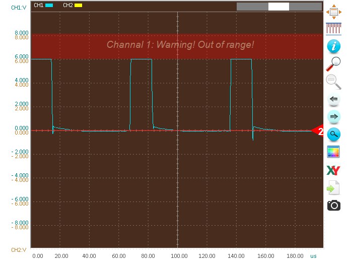
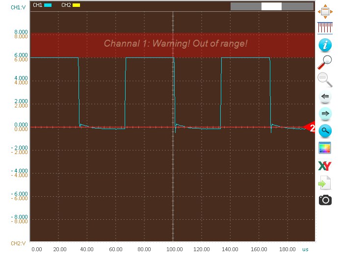
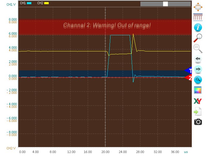
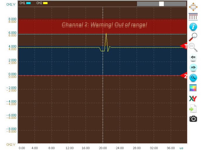
(using different dividers to avoid the 'out of range' warnings, 0.8 is actually 8.0 ZERO YOU STUPID AUTO-SMILEY B.S.)

../comfychair//scope/LED-withdiode.jpg

But again, as scary as that might be, I've used lights with these drivers without the diode extensively and haven't had anything croak yet. Is that another something that really should be addressed with a board redesign?

__________________

...


Online
Last seen: 3 min 1 sec ago
Title: ★★★★★
Joined: 11/27/2013
Posts: 4411
Location: Virginia, USA
comfychair wrote:[snip]If

comfychair wrote:
[snip]If it’s stable and doesn’t misbehave with just a single cap relocated, does the oscillation on Vcc hurt anything?

Thanks for testing – the results seem reasonable considering the other test results you’ve already shown. I don’t think the oscillation is going to hurt anything. Hopefully others will chime in one way or another. I would still like to move the diode & cap towards VCC, but no sense fooling with that until we’re reasonably sure of things.

I’m a little lost with the most recent trace. I see the spike, but I’m confused about the scales despite your explanation. It seems that the resting voltage of LED- shows up as 2v? And when the FET turns on LED- dips to 0v, and then spikes to >8v when the FET turns off?

I read some about margins recently. Apparently a 20% margin is normal for engineering. As in, if all the parts subjected to the spike can handle an 10v potential from LED- towards B+ (or whatever), then 8v would be OK.

comfychair's picture
Offline
Last seen: 1 year 10 weeks ago
Title: ★★★★★
Joined: 01/12/2013
Posts: 5873
That's with the probe on LED-

That's with the probe on LED- & ground clip to battery negative. I only changed the dividers to get rid of the out of range message. The waveform didn't change, just the voltage scale on the side.

By the way, what IS the proper connection to look at the signal to the LEDs?

__________________

...


Online
Last seen: 3 min 1 sec ago
Title: ★★★★★
Joined: 11/27/2013
Posts: 4411
Location: Virginia, USA
Sounds legit to me. Remember

Sounds legit to me. Remember I’ve got about the same experience with a scope as you Smile. Knowing where that clip goes is just part of keeping us on the same page.

Please try the same test with one probe on LED- and one probe on the FET’s tab (eg the other end of the wire that goes to LED-). I don’t understand well enough to know whether the spike should be worse there or not.

comfychair's picture
Offline
Last seen: 1 year 10 weeks ago
Title: ★★★★★
Joined: 01/12/2013
Posts: 5873
Well I dunno if this is

Well I dunno if this is normal for all oscilloscopes, but on this one grounding the clip on either probe provides ground for both of them. Nothing on screen changes if you have both clipped to ground and then remove either one.

Ground clip to LED-, probe to LED+?

Now that I think about how I had it connected, I think the trace is inverted... it looks almost like a mirror image of the gate signal.

__________________

...


WarHawk-AVG's picture
Offline
Last seen: 17 hours 16 min ago
Title: ★★★★★
Joined: 01/04/2014
Posts: 4873
Location: H-Town
OK…the BLFDD redesigns are in

OK…the BLFDD redesigns are in the works…Mattaus is currently reviewing, finalizing my tweakage of his builds and if they check out he will be re-releasing with the design suggestions you guys recommended

I hope I did him proud!

Ledsmoke's picture
Offline
Last seen: 10 weeks 2 days ago
Title: ★★★★★
Joined: 08/08/2011
Posts: 1989
Location: Denmark
Thank you all you guys. I

Thank you all you guys. I could never have figured any of this out by myself and yet I can follow most of the discussion guing on here. You guys are brilliant! TY Smile

__________________

~ Ledsmoke ~

Dutch humor:

djozz wrote:

 I do not think that the BLF-community benefits much from it except by making people uncertain now, who were thusfar quite happy about their light measurements Tongue Out.

I love this guy Smile

Cereal_killer's picture
Offline
Last seen: 8 weeks 4 days ago
Title: ★★★★★
Joined: 07/22/2013
Posts: 2955
Location: Columbus, OH USA Earth
comfychair wrote:If I want to

comfychair wrote:

../comfychair//scope/V2.jpg

If I want to do this with a zener mod would I replace the diode with the R200 resistor (like normal) and add the zener diode to the now empty C1 pads or does the zener diode have to also have the cap in the factory position?

__________________

Please help support my research by giving or sharing. GoFundMe.com/DansDrones


Always remember SPC Joey Riley, KIA 11/24/14.

Online
Last seen: 3 min 1 sec ago
Title: ★★★★★
Joined: 11/27/2013
Posts: 4411
Location: Virginia, USA
Cereal_killer

Cereal_killer wrote:

comfychair wrote:

If I want to do this with a zener mod would I replace the diode with the R200 resistor (like normal) and add the zener diode to the now empty C1 pads or does the zener diode have to also have the cap in the factory position?

We haven’t tested it (AFAIK), but the zener mod drivers simply do not have this problem (we assume). Build them as normal but do not bother with a gate resistor (use a jumper instead).

Specifically:

  • Without the reverse polarity protection diode there is no boost circuit, so the overvoltage condition does not exist
  • Without the reverse polarity diode in place the decoupling cap (C1) should act to smooth out any spikes generated on B+ by the FET switching.

Cereal_killer's picture
Offline
Last seen: 8 weeks 4 days ago
Title: ★★★★★
Joined: 07/22/2013
Posts: 2955
Location: Columbus, OH USA Earth
even with the AOD510 I can

even with the AOD510 I can get away with building them regular and no gate resistor?

thx

edit Sorry I wasnt asking a repetitive question here about the 510’s working in general, I got that, I have one together now on the bench with a 510- I was asking specifically about zener modded old style 17dd’s with the 510…

__________________

Please help support my research by giving or sharing. GoFundMe.com/DansDrones


Always remember SPC Joey Riley, KIA 11/24/14.

Online
Last seen: 3 min 1 sec ago
Title: ★★★★★
Joined: 11/27/2013
Posts: 4411
Location: Virginia, USA
Cereal_killer wrote:even with

Cereal_killer wrote:
even with the AOD510 I can get away with building them regular and no gate resistor?

thx

That’s definitely what I’m seeing at this point.

comfychair's picture
Offline
Last seen: 1 year 10 weeks ago
Title: ★★★★★
Joined: 01/12/2013
Posts: 5873
YES AOD510 WORKS WITH NO GATE

YES AOD510 WORKS WITH NO GATE RESISTOR* AFTER MOVING C1 TO B+/GND! All of them work with no gate resistor after moving the cap. Even the 15DD with the IRLM2502 works with no gate resistor after moving C1.

*replaced with a jumper on the versions with gate/pulldown pads, pulldown location left open, of course

__________________

...


WarHawk-AVG's picture
Offline
Last seen: 17 hours 16 min ago
Title: ★★★★★
Joined: 01/04/2014
Posts: 4873
Location: H-Town
I think I have a copy of the

I think I have a copy of the BLF15DD, I can re-design it like the BLF17DD is that is what you guys want

In fact, I might be able to make it single sided (nothing on the battery + side of the board)

Working on it now

Cereal_killer's picture
Offline
Last seen: 8 weeks 4 days ago
Title: ★★★★★
Joined: 07/22/2013
Posts: 2955
Location: Columbus, OH USA Earth
I’ve found some strange

I’ve found some strange behavior…

Since getting my 858D station yesterday I’ve built 6 17dd’s (5 this new way and one zener modded), 3 of them with the AOD510’s and 2 with the old Vishay’s are working fine however the one with the one FET I have out of an M6 is giving me some issues with the exact same firmware. It’s heving problems when cycling threw the modes, after turbo sometimes it’ll miss moonlight completely and just go back to low (5-mode off-time with no memory and moon defaulted on without the star needing to be soldered), other times it will go to moon but with a bad preflash.

I’m not really complaining, I have exactly one of these FET’s and dont really mind discarding it to the random parts drawer, just reporting my findings.

__________________

Please help support my research by giving or sharing. GoFundMe.com/DansDrones


Always remember SPC Joey Riley, KIA 11/24/14.

comfychair's picture
Offline
Last seen: 1 year 10 weeks ago
Title: ★★★★★
Joined: 01/12/2013
Posts: 5873
What's the p/n on the problem

What's the p/n on the problem FET? Curious to find a datasheet on it and see what it has in the section for gate characteristics. Both the 70N02 & AOD510 have a total gate charge number known to be something the attiny is capable of driving. Above something like Qg=40 they can get troublesome, or at least that's the general number I've heard to stay under.

__________________

...


Cereal_killer's picture
Offline
Last seen: 8 weeks 4 days ago
Title: ★★★★★
Joined: 07/22/2013
Posts: 2955
Location: Columbus, OH USA Earth
DTU 30N02 DD22U then a

DTU
30N02
DD22U

then a little circle symbol with an Lv

__________________

Please help support my research by giving or sharing. GoFundMe.com/DansDrones


Always remember SPC Joey Riley, KIA 11/24/14.

Online
Last seen: 3 min 1 sec ago
Title: ★★★★★
Joined: 11/27/2013
Posts: 4411
Location: Virginia, USA
Clear PCB images are here

Clear PCB images are here that show the FET’s markings and M6 layout: Supfire M6 – resistor mod

comfychair's picture
Offline
Last seen: 1 year 10 weeks ago
Title: ★★★★★
Joined: 01/12/2013
Posts: 5873
Wow that thing is awful.

Wow that thing is awful. Throw it away. Rds(on) is around 0.030 ohms, 70N02 under the same conditions is 0.004-0.006. lol

__________________

...


Rufusbduck's picture
Offline
Last seen: 11 hours 12 min ago
Title: ★★★★★
Joined: 04/04/2012
Posts: 7482
Location: Golden state
This is really great stuff

This is really great stuff you’ve found out CC and precisely the kind of thing that only comes out after new ideas are tried out and someone takes the time to troubleshoot odd behavior. Good job.

__________________

Three Tanna leaves to give him life, nine to give him movement. But what if he eats the whole bag?

Scott

Cereal_killer's picture
Offline
Last seen: 8 weeks 4 days ago
Title: ★★★★★
Joined: 07/22/2013
Posts: 2955
Location: Columbus, OH USA Earth
wight wrote:Cereal_killer

wight wrote:
Cereal_killer wrote:

comfychair wrote:

If I want to do this with a zener mod would I replace the diode with the R200 resistor (like normal) and add the zener diode to the now empty C1 pads or does the zener diode have to also have the cap in the factory position?

We haven’t tested it (AFAIK), but the zener mod drivers simply do not have this problem (we assume). Build them as normal but do not bother with a gate resistor (use a jumper instead).

Specifically:

  • Without the reverse polarity protection diode there is no boost circuit, so the overvoltage condition does not exist
  • Without the reverse polarity diode in place the decoupling cap (C1) should act to smooth out any spikes generated on B+ by the FET switching.

So as it turns out the zener modded driver do in fact have the issue, I of course dont have a scope to know if its the very same issue but it was giving me identical behavior where it skipped modes or shut its self down or just overall acted bad when I tried building it with R3 jumpered and C1 populated like normal (with the 10uf cap and the zener diode) and a R200 in place of the protection diode and it did turn on but neither luxdrv fast or phase correct (its known that fet drivers still need luxdrv to run at phase correct PWM) nor my custom weapon mounted UI were usable with it like that. This is in my MT-G2 ZY-T08.
Took it back apart replaced the jumper at R3 with a 130 and populated R4 with a 10k and the light worked perfect with both FW’s!

Brings back the question, can I put the zener diode on the C1 pad with no C1 and put the 10uf cap from batt+ to like with the non-zener ones or does the zener diode REQUIRE the cap to be there?

__________________

Please help support my research by giving or sharing. GoFundMe.com/DansDrones


Always remember SPC Joey Riley, KIA 11/24/14.

comfychair's picture
Offline
Last seen: 1 year 10 weeks ago
Title: ★★★★★
Joined: 01/12/2013
Posts: 5873
Cereal_killer wrote:(its

Cereal_killer wrote:
(its known that fet drivers still need luxdrv to run at phase correct PWM)

Most certainly not the case! Only the momentary switch firmwares, that use a different 'sleep' method, require phase correct FW (and that holds true whether it's a FET or 7135s). I built many many lights with FET drivers running luxdrv converted to fast-PWM.

The zener and the cap aren't directly related, they just got piggybacked because they both required connections to the same points. If moving the cap fixes it (which I doubt, since without the normal diode at D1 there is no longer a voltage boosting situation) then that's fine.

__________________

...


Cereal_killer's picture
Offline
Last seen: 8 weeks 4 days ago
Title: ★★★★★
Joined: 07/22/2013
Posts: 2955
Location: Columbus, OH USA Earth
Can I send you the exact .c

Can I send you the exact .c and hex files I have for luxdrv? When I try changing it to fast and putting it on any of the FET drivers it doesn’t run, or can you send me your file so I can try it?

Fast or slow will work on my 105c (and other 7135 drivers) but this version luxdrv fastPWM doesn’t work on my FET drivers.

Currently the light is running with all resistor pads populated and slowPWM and it didn’t run with R3 jumpered. Ignoring for a second the FW issue fast vs. slow, what should I do with it, leave it as-is or move the cap down to where I am using for 3v ones (your v2 pic) and re-jumper R3?

__________________

Please help support my research by giving or sharing. GoFundMe.com/DansDrones


Always remember SPC Joey Riley, KIA 11/24/14.

comfychair's picture
Offline
Last seen: 1 year 10 weeks ago
Title: ★★★★★
Joined: 01/12/2013
Posts: 5873
../comfychair//driverhac

../comfychair//driverhacks/nanjg-092/ld-fastpwm/

Strobe & ramping deleted, still has memory & battery monitor/beacon mode. Levels are 255, 90, 12, 3.

__________________

...


Ledsmoke's picture
Offline
Last seen: 10 weeks 2 days ago
Title: ★★★★★
Joined: 08/08/2011
Posts: 1989
Location: Denmark
@ CC: Your are my hero. And

@ CC: Your are my hero. And every other modder wanting to be mean to led lights. I never would have thought about getting this heavy into the electronic part of the hobby if it was not for you. TY Smile

__________________

~ Ledsmoke ~

Dutch humor:

djozz wrote:

 I do not think that the BLF-community benefits much from it except by making people uncertain now, who were thusfar quite happy about their light measurements Tongue Out.

I love this guy Smile

Online
Last seen: 3 min 1 sec ago
Title: ★★★★★
Joined: 11/27/2013
Posts: 4411
Location: Virginia, USA
Cereal_killer wrote:Can I

Cereal_killer wrote:
Can I send you the exact .c and hex files I have for luxdrv? When I try changing it to fast and putting it on any of the FET drivers it doesn’t run, or can you send me your file so I can try it?

Fast or slow will work on my 105c (and other 7135 drivers) but this version luxdrv fastPWM doesn’t work on my FET drivers.

Currently the light is running with all resistor pads populated and slowPWM and it didn’t run with R3 jumpered. Ignoring for a second the FW issue fast vs. slow, what should I do with it, leave it as-is or move the cap down to where I am using for 3v ones (your v2 pic) and re-jumper R3?

Either move the cap or add one where you described.

Offline
Last seen: 1 hour 57 min ago
Title: ★★
Joined: 01/31/2015
Posts: 178
Location: Atlanta
?

does anybody happen to have screen shots or images that were posted by comfychair? trying to learn more about the whole C1 cap placement decision on the current iterations of the BLF 17DD.

FmC
FmC's picture
Offline
Last seen: 7 hours 24 min ago
Title: ★★★★★
Joined: 03/31/2013
Posts: 1385
Location: AU
seasam wrote:does anybody

seasam wrote:
does anybody happen to have screen shots or images that were posted by comfychair? trying to learn more about the whole C1 cap placement decision on the current iterations of the BLF 17DD.


Is this what you are after?


__________________


Offline
Last seen: 1 hour 57 min ago
Title: ★★
Joined: 01/31/2015
Posts: 178
Location: Atlanta
FmC wrote:seasam wrote:does

FmC wrote:

seasam wrote:
does anybody happen to have screen shots or images that were posted by comfychair? trying to learn more about the whole C1 cap placement decision on the current iterations of the BLF 17DD.


Is this what you are after?

thanks that does help me with the history. I was specifically curious about how noisy the Vcc line gets with the current C1 cap placement since the screenshots are missing. From what I can tell in the comments of this thread there may be noise/spikes with the current C1 cap placement but it was deemed acceptable. Also, I’m still wondering why the gate resistor was deleted if it could have helped with the spikes as well. Guess I need a scope and more studying Party

I’ve been having an issue with a driver built from a wight board running star firmware. When running a triple XPL at high current I’ve been having issues with the driver flickering and shutting down. High current being bypassed springs with LG HE2 cells. Nonbypassed springs or tamer cells don’t seem to have this problem so I was looking here for clues Big smile

I need a scope…

FmC
FmC's picture
Offline
Last seen: 7 hours 24 min ago
Title: ★★★★★
Joined: 03/31/2013
Posts: 1385
Location: AU
That’s interesting, I’m

From memory, the revised C1 placement cleaned up the spike greatly.

That’s interesting, I’m having the same problem with one of the 17mm DD MTN drivers, which is pretty much the same as Wight’s board.

Does your problem driver also switch off if you run it on low for a few seconds?

I know the design of these boards are proven, as there are hundreds of them out there, & I’ve built plenty before this one, but it’s still a pain when you can’t put your finger on a particular issue…

__________________


Tom E's picture
Online
Last seen: 12 min 50 sec ago
Title: ★★★★★
Joined: 08/19/2012
Posts: 6338
Location: LI NY
Weird - I'm using a wight

Weird - I'm using a wight FET+1*7135 driver with the SIR800DP in a triple XPL X6 getting 10 amps with all heavy bypass wires, etc. Basically works well but I got one noticeable issue and it's a blink when changing modes to moon mood, fron turbo or not. RMM recommended trying a resisotr off the FET gate, like a 100K or so -- didn't try that yet.

Offline
Last seen: 1 hour 57 min ago
Title: ★★
Joined: 01/31/2015
Posts: 178
Location: Atlanta
FmC wrote:From memory, the

FmC wrote:
From memory, the revised C1 placement cleaned up the spike greatly.

That’s interesting, I’m having the same problem with one of the 17mm DD MTN drivers, which is pretty much the same as Wight’s board.

Does your problem driver also switch off if you run it on low for a few seconds?

I know the design of these boards are proven, as there are hundreds of them out there, & I’ve built plenty before this one, but it’s still a pain when you can’t put your finger on a particular issue…

yeah the problem will happen in low it will flicker a bit and then shut off a lot of times. really only in a high current situation though. I can’t remember if it was medium and high too, but definitely low.

my parts are from RMM so I think this driver is a NXP PSMN2R4-30YLDX FET. have some SIR800DP but haven’t tried those yet. I don’t think the FET choice is an issue though.

Tom E wrote:

Weird - I’m using a wight FET+1*7135 driver with the SIR800DP in a triple XPL X6 getting 10 amps with all heavy bypass wires, etc. Basically works well but I got one noticeable issue and it’s a blink when changing modes to moon mood, fron turbo or not. RMM recommended trying a resisotr off the FET gate, like a 100K or so — didn’t try that yet.

funny you should mention the gate resistor because that did seem to be a good thing from this discussion, so I was trying to understand why it was removed from the design in the first place. parts count reasons?

I actually added a 200ohm resistor (replaced the existing diode) and a zener along with a second 10uF cap in parallel with the zenner (also all known as the zener mod – but still running as single cell). C1 still has 10uF cap as well. This was discussed earlier in the thread as a possibility of smoothing out the Vcc line.

To be honest I haven’t been able to get my light to act up again after doing the zener mod with this single cell driver. It was pretty easy to reproduce the behavior before I added the zener. I would like to try the gate resistor at some point too (without the zener). I will probably build another driver and keep tinkering. I’ll update if my driver acts up again.

Tom E's picture
Online
Last seen: 12 min 50 sec ago
Title: ★★★★★
Joined: 08/19/2012
Posts: 6338
Location: LI NY
It was removed because it did

It was removed because it did nothing to have it there, at the time. I was involved in the FET drivers early on, when comfy was leading us to the FET farm, FET fame, FET nirvana, errr something like that... I l think the theory of the resistor was good, but practically had no effect. I've built a lot of FET drivers up, from Nanjg's at first, then the OSHPark versions of the BLF DD 1.0, C_K's, and wights. Never seen a problem til this little blink issue - all 3 FET+1x7135 wight drivers I built have it.

ToyKeeper's picture
Offline
Last seen: 12 hours 31 min ago
Title: ★★★★★
Joined: 01/12/2013
Posts: 3635
Location: n., a point or extent in space
I’m tempted to see if I can

I’m tempted to see if I can salvage any of the old pics from this thread from archive.org or other caches. I found the data very useful, and would like to be able to refer to it again in the future.

Offline
Last seen: 1 hour 57 min ago
Title: ★★
Joined: 01/31/2015
Posts: 178
Location: Atlanta
Tom E wrote:It was removed

Tom E wrote:

It was removed because it did nothing to have it there, at the time. I was involved in the FET drivers early on, when comfy was leading us to the FET farm, FET fame, FET nirvana, errr something like that… I l think the theory of the resistor was good, but practically had no effect. I’ve built a lot of FET drivers up, from Nanjg’s at first, then the OSHPark versions of the BLF DD 1.0, C_K’s, and wights. Never seen a problem til this little blink issue – all 3 FET+1×7135 wight drivers I built have it.

lol FET nirvana. Gotcha, well thanks for clearing up the history a bit. I appreciate your insight on this, especially since you’ve probably built a million more drivers than I have Big smile Please be sure to post any updates, I would be interested to hear what you find.

ToyKeeper wrote:
I’m tempted to see if I can salvage any of the old pics from this thread from archive.org or other caches. I found the data very useful, and would like to be able to refer to it again in the future.

yeah I tried wayback but that didn’t seem to work. that info sure would be useful.

Tom E's picture
Online
Last seen: 12 min 50 sec ago
Title: ★★★★★
Joined: 08/19/2012
Posts: 6338
Location: LI NY
comfy had some great ref

comfy had some great ref material - illustrated pics, drawings, etc. Boy, hope you can find backups - that would be great.

RMM
RMM's picture
Offline
Last seen: 2 hours 51 min ago
Title: ★★★★★
Joined: 07/23/2013
Posts: 3325
Location: USA
FmC wrote:From memory, the

FmC wrote:
From memory, the revised C1 placement cleaned up the spike greatly. That's interesting, I'm having the same problem with one of the 17mm DD MTN drivers, which is pretty much the same as Wight's board. Does your problem driver also switch off if you run it on low for a few seconds? I know the design of these boards are proven, as there are hundreds of them out there, & I've built plenty before this one, but it's still a pain when you can't put your finger on a particular issue...

I've never seen one of the [properly built] MTN drivers glitch up, not once.  You're not running zener mod, right?

__________________

Mountain Electronics : batteries, Noctigon, and much more! What's new?  Garage Sale

FmC
FmC's picture
Offline
Last seen: 7 hours 24 min ago
Title: ★★★★★
Joined: 03/31/2013
Posts: 1385
Location: AU
RMM wrote:I’ve never seen one

RMM wrote:
I’ve never seen one of the [properly built] MTN drivers glitch up, not once.  You’re not running zener mod, right?

No, not doing the zener build.

I was hoping you were reading this thread, in case you had come across a similar issue, & could point me in the right direction of what may be the cause.

I’m using the components (resistors, cap, 13a, diode) from new Nanjg’s, & the board & fet were from your store.

The only component I haven’t swapped out on the problem board is the fet, so that may well be the answer.

__________________


RMM
RMM's picture
Offline
Last seen: 2 hours 51 min ago
Title: ★★★★★
Joined: 07/23/2013
Posts: 3325
Location: USA
Hmm, I don't think it would

Hmm, I don't think it would be the FET.  Maybe the Nanjg's capacitor isn't up to snuff.  I would suspect that first.

__________________

Mountain Electronics : batteries, Noctigon, and much more! What's new?  Garage Sale

Comment viewing options

Select your preferred way to display the comments and click "Save settings" to activate your changes.